![]()
 |
||||||||||||||||||||
Hardware Design
Although our main emphasis is on FPGA design and development we have a good background in digital design and very close contacts with a local Analogue design consultant who advises on any critical analogue design issues. It has transpired that few customers require pure FPGA development, most of our work involves developing complete solutions for customers designing the hardware to support FPGA functionality.
We have completed a couple of complete custom product developments and have advised many customers on hardware aspects of their planned developments.We have experience of 32/16 and 8 bit microprocessor design, for example a design with dual bus masters one an Intel device (with Intel 'std' control signals), the other a Motorola (with Motorola 'std' control signals), with a processor clock speed of 40MHz.
Other designs have incorporated PCI, USB, ISA SPI, I2C interfaces, ADC and DAC convertors etc.
We have software tools to allow multi layer surface mount boards to be designed, from schematic capture to layout. We can mount any packages up to BGA in house. Contacts with a local company specializing in small run prototype manufacture allow fast prototype/evaluation boards (with BGA technology) to be designed and built.We are currently developing several hardware based customer products, more details to follow as we are able to release them.
A few examples of hardware we have developed are shown below. This web site is being re-designed, further examples will be included in the re-vamped site.
Custom Product DesignCustom Board Design
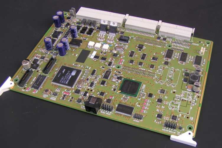
This board is one of several used in a client's product.
The board contains a Cirrus Arm CPU, Cyclone II FPGA, a 5A 48V motor drive, a +/- 12V 500mA motor drive, stepper drivers, digital IO, analogue sensing inputs, on-board temperature sensors, system thermistor inputs and an ethernet link to another board. This client uses a third party for PCB design but we guided component placement and did the entire placement and routing of the three switching power supplies with very satisfactory results. This is a fairly cost sensitive board so audio drivers were used on the +/- 12V motor output. This saved these have been performed well in all testing.
The FPGA design was split with one of the customers engineers who had experience driving the motor output, we implemented all the other functionality.
Customer Product Design 1
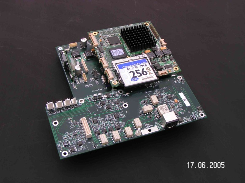
This is part of the electronics board stack we developed as part of a complete customer product design. This stack fits in a compact 1U enclosure and is based on an Cyclone FPGA based motherboard upon which the Single Board Computer and the analogue interface board sit. There are a couple more peripheral boards that interface with the motherboard.
Customer Product Design 2
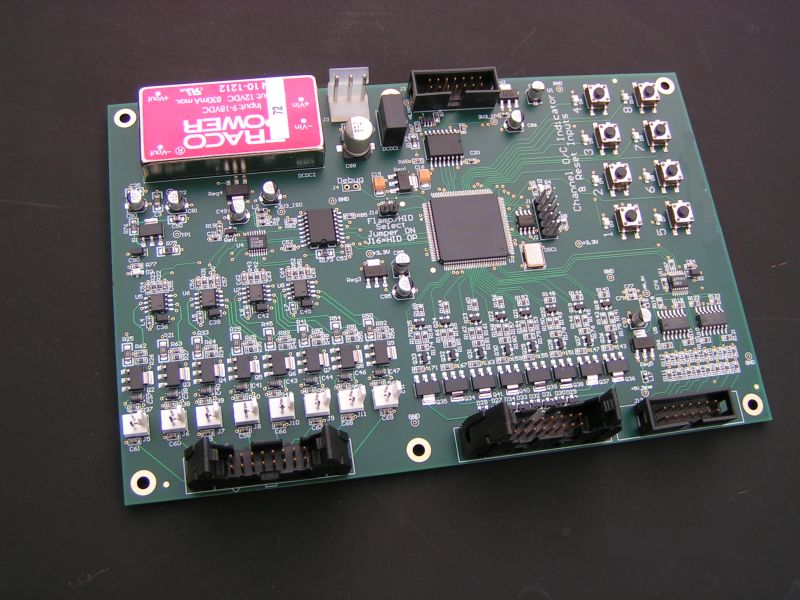
This is an ongoing complete ground up industrial product design for a client. The product requires various different interface boards controlled from a central controller. Final I/O functional requirements were not defined when this design was started so all I/O boards have been based around FPGAs for flexibility. The communications between the various boards are via proprietary serial interfaces, with differential clocking for reliability. This has proven to be a flexible approach as the system requirements developed.
The board below is part of this large system and provides isolated control outputs and monitoring inputs with fault indication LEDs and reset switch inputs.
EASY PCI Interface board
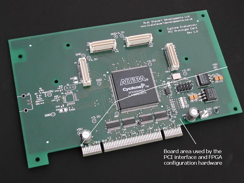
We have developed our EASY PCI interface board and core based on Altera's low cost Cyclone FPGA family. Developing a custom PCI interface board with any amount of custom logic is not a trivial task. There are currently two possibilities, use a commercial PCI interface core in an FPGA or use a bridge IC and an FPGA. Commercial cores can cost thousands of dollars (an example is Altera's 32bit 33MHz Master/Target core is $9K, target only $4K) and using additonal devices to implement a PCI bridge make board design/build more complex and costly. There doesn't seem to be a simple, reasonably priced route for those who want to quickly implement a PCI interface board, whether for prototyping of production.
As you can see below, the board contains a Cyclone 1C6 FPGA, an EPCS4 configuration device, power regulators and headers to allow access to all pins not associated with the PCI interface. The board itself can be used for prototyping by connecting mezannine boards to the headers, or it can be used as the basis for bespoke boards by adding custom hardware/FPGA design. The board can operate stand alone on the bench when powered from a 5V supply.
A 3.3V surface mount crystal is included, connected to PLL2 to allow internal logic to be run at speeds of 20MHz * M/(N * post_scale_counter) where M = 2 to 32, N and post_scale_counter = 1 to 32.
The PCI interface core for the FPGA is initially a Target only core. The core has been designed to be as simple as possible to interface to and will be competitively priced, the price dependant on volume.
The Cyclone 1C6 costs < $15 in low volumes, so it will be seen that this will a very cost effective route for clients to implement custom PCI interface card design.
The base PCI interface board can be seen here.
Our tests have shown the basic PCI functionality and interrupt support of the board and the core to be working well (these were actually 'right first time' when we worked out what the operating system was up to). We are now investigating driver and example software development and preparing for board manufacture.
The EASY PCI core has been designed to be as simple as possible to interface to and has proved very easy to P+R, easily meeting the required PCI timing constraints and using <400 logic elements.
A Core and Board design description which describes core implementation details, performance, compliance is now available (right click and 'Save Target As' to download it in Windows).
The circuitry outside the marked area was included to allow board debug/evaluation. This can be quickly removed for custom board development. It can be seen that there is a significant amount of space on the board to allow rapid custom prototypes to be developed using this as a basis.
Although our main background is in digital hardware design, we have good professional contacts with several experienced analogue design and software engineers on whom we can call if an application requires extensive expertise in these areas.As a member of the Professional Contractors Group (PCG) we have access to 12,000 Engineering and IT contracting specialists and so can source experienced Engineers in almost any area of Engineering or IT.
| Copyright © Nial Stewart Developments Limited |
Site design: EverWebbey
Solutions
|